RT-793/ASQ
(Part of AN/ASQ-19 & AN/ASQ-88)
How to get it working with a 115V 3Ph 400 Hz supply.
How to get it working with a 115V 3Ph 400 Hz supply.
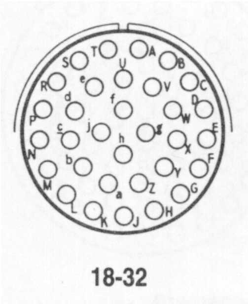
Connectors for the control head MS3116-18-32-S-W
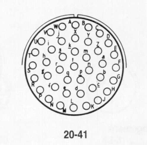
(Note: W means that the connector is rotated). The one showed here IS NOT rotated.MS3115-20-41-S
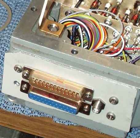
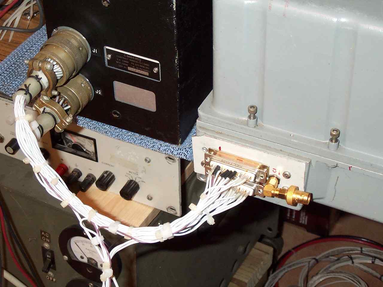
The mating connector for the RT is unavailable or very expensive. It can be easily replaced with 2 DB-25s and an SMA for the antenna. I suggest to connect the two DB-25 to FL-1. To avoid confusion, the DB-25 male will be called DJ-1 and the female DP-1.
Can't find the MS3116 connectors? Let me know and I'll try to help you out.
| Signal | Control Head | RT-793 FL1 | RT-793 DB-25s |
| 200/300 MHz | J1-Z | FL1-44 | DP-19 |
| 10 MHz BCD 8 | J1-Y | FL1-31 | DP-10 |
| 10 MHz BCD 4 | J1-X | FL1-54 | DP-25 |
| 10 MHz BCD 2 | J1-L | FL1-43 | DP-18 |
| 10 MHz BCD 1 | J1-K | FL1-33 | DJ-14 |
| 1 MHz BCD 8 | J1-J | FL1-26 | DP-5 |
| 1 MHz BCD 4 | J1-H | FL1-27 | DP-6 |
| 1 MHz BCD 2 | J1-G | FL1-28 | DP-7 |
| 1 MHz BCD 1 | J1-F | FL1-29 | DP-8 |
| 0.1 MHz BCD 8 | J1-E | FL1-39 | DP-14 |
| 0.1 MHz BCD 4 | J1-D | FL1-40 | DP-15 |
| 0.1 MHz BCD 2 | J1-C | FL1-41 | DP-16 |
| 0.1 MHz BCD 1 | J1-B | FL1-42 | DP-17 |
| 0.00/0.05 MHz | J1-A | FL1-32 | DP-11 |
| +28VDC | J1-u | ||
| 115V Ph A | FL1-4 | DJ-8 | |
| 115V Ph B | FL1-6 | DJ-7 | |
| 115V Ph C | FL1-8 | DJ-6 | |
| +28VDC | J1-W | ||
| +28VDC | J2-W | ||
| Audio Output to 600 ohm speaker | J1-P | ||
| On/Off | J2-D | FL1-20 | DJ-20 |
| On/Off Return | J2-Y | GND | DJ-4 |
| Guard On/Off | J2-X | FL1-21 | DJ-19 |
| Guard On/Off return | J2-A | GND | DJ-2 |
| Audio In | J1-N | FL1-35 | DP-3 |
| Audio Out (to speaker 600 ohm) | J1-j | ||
| Audio Out (to speaker 600 ohm GND) | J1-P | ||
| Squelch Disable | J2-a | FL1-48 | DP-22 |
| Squelch Disable Return | J2-y | ||
| Jumper | J2-N and J2-c | ||
| GND | J1-M | GND | DP-12 |
| J1-e | GND | DP-13 | |
| J2-W | |||
| J2-d | FL1-12 | DJ-11 | |
| J1-r | FL1-12 | DJ-12 | |
| +28VDC | FL1-12 | DJ-10 | |
| FL1-1 | DJ-9 | ||
| FL1-9 | DJ-24 | ||
| FL1-10 | DJ-25 | ||
| FL1-11 | DJ-13 | ||
| FL1-17 | DJ-23 | ||
| FL1-18 | DJ-22 | ||
| FL1-19 | DJ-21 | ||
| FL1-22 | DJ-18 | ||
| FL1-23 | DJ-17 | ||
| FL1-24 | DJ-16 | ||
| FL1-24 | DP-4 | ||
| FL1-30 | DP-9 | ||
| FL1-34 | DJ-15 | ||
| FL1-36 | DP-2 | ||
| FL1-38 | DP-1 | ||
| FL1-45 | DP-20 | ||
| FL1-46 | DP-21 | ||
| FL1-49 | DP-23 | ||
| FL1-53 | DP-24 | ||
| GND | DJ-1 | ||
| GND | DJ-3 | ||
| GND | DJ-5 |
| 28 VDC | J12-11, J8-1, J10-1, J10-11, J10-12, J5-8, J4-8, J7-3, J6-8, J6-11, J2-6, J2-9, J3-5, J3-11 |
| 6.6 VDC | J5-1, J5-3, J5-6, J6-1, J1-7 |
| 13.7 VDC | J5-7, J6-3, J6-13 |
| 20.7 VDC | J6-4 |
| 220 VDC | J5-4, J6-2, J6-5, J1-3 |
| -6 VDC | J6-6 |
Notes:
1)Voltages are measured without any module plugged in.
2)Measured voltages maybe higher
3)28VDC is present on J7-3 only when Guard Channel is turned on.
| Signal | Connector Converter Frequency Static J-12 | Connector Mechanical Tuner J-10 |
| 10 MHz BCD 8 Input | J12-12 (input) | |
| 10 MHz BCD 4 Input | J12-13 (input) | |
| 10 MHz BCD 2 Input | J12-14 (input) | |
| 10 MHz BCD 1 Input | J12-15 (input) | |
| 1 MHz BCD 8 Input | J12-6 (input) | |
| 1 MHz BCD 4 Input | J12-7 (input) | |
| 1 MHz BCD 2 Input | J12-8 (input) | |
| 1 MHz BCD 1 Input | J12-9 (input) | |
| 0.1 MHz BCD 8 Input | J12-1 (input) | |
| 0.1 MHz BCD 4 Input | J12-2 (input) | |
| 0.1 MHz BCD 2 Input | J12-3 (input) | |
| 0.1 MHz BCD 1 Input | J12-4 (input) | |
| 300-A | J10-8 (input) | |
| 200-B | J12-36 (output) | J10-2 (input) |
| 10-E | J12-34 (output) | J10-5 (input) |
| 10-D | J12-33 (output) | J10-4 (input) |
| 10-C | J12-32 (output) | J10-3 (input) |
| 10-B | J12-31 (output) | J10-7 (input) |
| 10-A | J12-30 (output) | J10-6 (input) |
| 1-E | J12-29 (output) | J10-10 (input) |
| 1-D | J12-28 (output) | J10-9 (input) |
| 1-C | J12-27 (output) | J10- (input) |
| 1-B | J12- (output) | J10- (input) |
| 1-A | J12-25 (output) | J10- (input) |
| 0.1-E | J12-24 (output) | J10-23 (input) |
| 0.1-D | J12-23 (output) | J10-21 (input) |
| 0.1-C | J12-22 (output) | J10-20 (input) |
| 0.1-B | J12-21 (output) | J10-19 (input) |
| 0.1-A | J12-20 (output) | J10-18 (input) |
| Signal | Control Head | RT-793 FL1 | RT-793 Modules |
| 200/300 MHz | J1-Z | FL1- | J12-17 |
| 10 MHz BCD 8 | J1-Y | FL1- | J12-12 |
| 10 MHz BCD 4 | J1-X | FL1- | J12-13 |
| 10 MHz BCD 2 | J1-L | FL1- | J12-14 |
| 10 MHz BCD 1 | J1-K | FL1- | J12-15 |
| 1 MHz BCD 8 | J1-J | FL1- | J12-6 |
| 1 MHz BCD 4 | J1-H | FL1- | J12-7 |
| 1 MHz BCD 2 | J1-G | FL1- | J12-8 |
| 1 MHz BCD 1 | J1-F | FL1- | J12-9 |
| 0.1 MHz BCD 8 | J1-E | FL1- | J12-1 |
| 0.1 MHz BCD 4 | J1-D | FL1- | J12-2 |
| 0.1 MHz BCD 2 | J1-C | FL1- | J12-3 |
| 0.1 MHz BCD 1 | J1-B | FL1- | J12-4 |
| 0.00/0.05 MHz | J1-A | FL1-32 | J2-10 |
| J8-1 | |||
| J8-2 | |||
| J8-3 | Output | -12VDC | |
| J8-4 | Output | 220 VDC | |
| J8-5 | |||
| J8-6 | Output | -6VDC | |
| J8-7 | |||
| J8-8 | Output | 460VDC | Not required ** |
| J8-9 | GND | ||
| J8-10 | |||
| J8-11 | Input | 115V 400Hz Ph 1 | |
| J8-12 | Input | 115V 400Hz Ph 2 | |
| J8-13 | |||
| J8-14 | Input | 115V 400Hz Ph 3 | |
| J8-15 | Return | GND |
** 460VDC is not required for receiver only operation.
Similarities and Differences Between the ARC-51BX and RT-793 The AN/ARC-51BX utilizes some modules that seem to be functionally equivalent to the one used on the RT-793.
- The 51BX does not utilize the Converter Frequency Static, since the control head interfaces directly to the Mechanical Tuner.
- The 51BX Power Supply A8 is not compatible without major modifications of the RT-793 mainframe. Utilizing the ARC-51 power supply module has the advantage of requiring one supply voltage only (28VDC). This modification will be discussed at a later time.
Disclaimer: In the preparation of these web pages, every effort has been made to offer the most current, correct and clearly expressed information possible. Nonetheless, inadvertent errors can occur. Users of the information contained or referenced on this site assume all risk of loss arising from any errors, omissions, inaccuracies, or changes in the information and also all risk of loss arising from any error.